The ESONN summer school is giving me - a theorist - the rather rare opportunity to be in a real-life laboratory and to take measurements. In that spirit, David and I spent two days learning the theory about, modelling the behaviour of, and directly probing the characteristics of metal-oxide-semiconductor field-effect transistors (MOSFETs). These devices take advantage of the physics of doped semiconductor materials to create electrical gates, which go on to form the basis of almost all traditional electronic devices. The MOSFET is the "most widely manufactured device in history, with an estimated total of 13 sextillion (1.3 × 10^22) MOS transistors manufactured between 1960 and 2018." (1)
The first day saw us learn to use software built to simulate how a device would behave upon inputting many fabrication processes and parameters and implementing them.

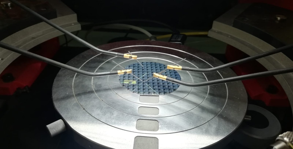
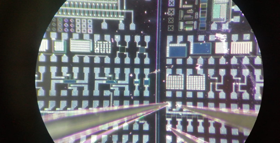
The world is not the same as a computer (as far as we know) so it is important to test fabricated devices in real life too - the simulations are only as good as the approximations in the models that go into the software. The next day we had the chance to test devices using a probe station applying different drain and gate voltages, as shown below.

Credit to David for the photos and the help in the lab!


Commentaires